PCB Design
Designing a PCB from scratch in KiCad
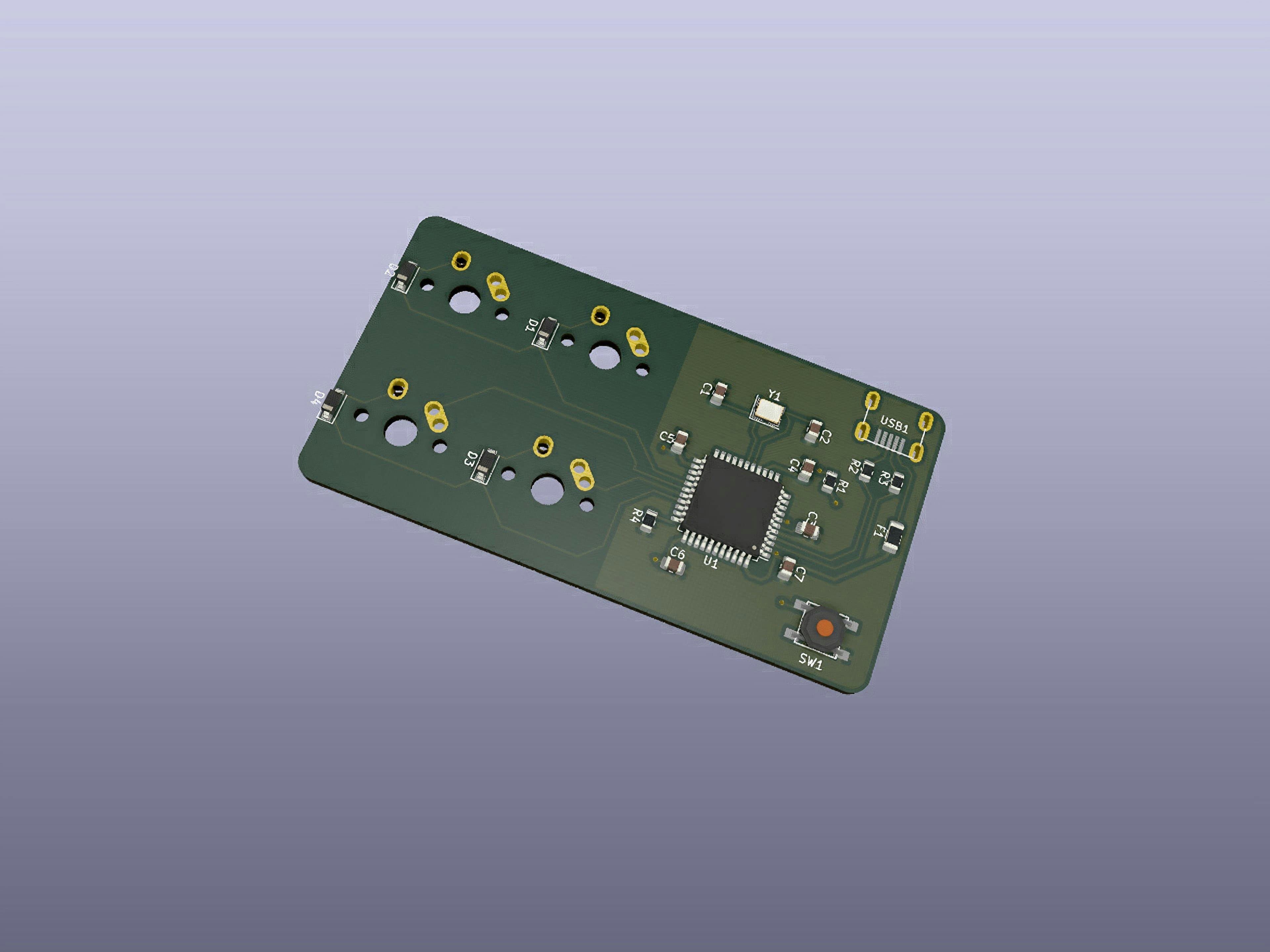
Designing electronics is an essential skill for a designer who is practices in crafting digital user experiences. Consequently, I wanted to broaden my technical realization capabilities and thus, I embarked on a journey of creating my very own Printed Circuit Board (PCB). I was curious to explore how I could use my knowledge of datasheets and components to make a neat PCB. I had heard about a macro pad, a device with a few buttons that can be connected to a computer to act as an extension of a keyboard, and thought this would be a great project to challenge myself.
In this mini project, I had the opportunity to learn how to use the KiCad schematics editor. By familiarizing myself with this tool, I was able to gain a better understanding of how to find digitalized components, and how to connect them in a schematic to ultimately design and edit a PCB layout. The rendered result of the macro pad PCB can be seen in the image above.